| Price | Negotiation |
| MOQ | 1 package |
| Delivery Time | 3-5 work days |
| Certification | Original Parts |
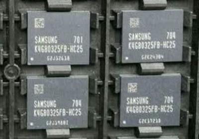
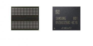
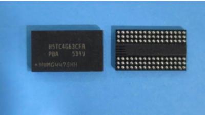
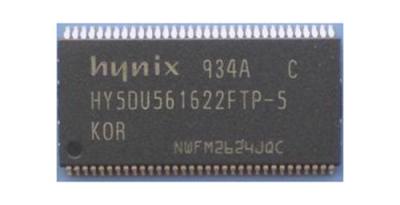
| Model Number | HY5DU561622FTP-5 |
| Packaging Details | 10cm X 10cm X 5cm |
| Payment Terms | T/T, PayPal, Western Union, Escrow and others |
| Supply Ability | 6000pcs per month |
| Packaging Details | 10cm X 10cm X 5cm | Item number | HY5DU561622FTP-5 |
| Volt | 2.4V | Model Number | HY5DU561622FTP-5 |
| Supply Ability | 6000pcs per month | Certification | Original Parts |
| Payment Terms | T/T, PayPal, Western Union, Escrow and others | Memory Denity | 256Mb |
| Data Rate | 200MHz | Price | Negotiation |
| Delivery Time | 3-5 work days | Temp. | 0 °C~70 °C |
| Minimum Order Quantity | 1 package | Package | 66 TSOP |
HY5DU561622FTP-5 DRAM Memory Chip SDRAM Memory 256Mbit Surface Mount, 200MHz, 2.4 → 2.7 V
| Attribute | Value |
|---|---|
| Memory Size | 256Mbit |
| Organisation | 16M x 16 bit |
| Data Rate | 200MHz |
| Data Bus Width | 16bit |
| Number of Bits per Word | 16bit |
| Number of Words | 16M |
| Mounting Type | Surface Mount |
| Package Type | TSOP |
| Pin Count | 66 |
| Dimensions | 22.33 x 10.26 x 1.044mm |
| Height | 1.044mm |
| Length | 22.33mm |
| Minimum Operating Supply Voltage | 2.4 V |
| Minimum Operating Temperature | 0 °C |
| Maximum Operating Temperature | +70 °C |
| Maximum Operating Supply Voltage | 2.7 V |
| Width | 10.26mm |
DESCRIPTION
The
Hynix
HY5DU561622FTP-5,
-4
series
are
a
268,435,456-bit
CMOS
Double
Data
Rate(DDR)
Synchronous
DRAM,
ideally
suited
for
the
point-to-point
applications
which
requires
high
bandwidth.
The
Hynix
16Mx16
DDR
SDRAMs
offer
fully
synchronous
operations
referenced
to
both
rising
and
falling
edges
of
the
clock.
While
all
addresses
and
control
inputs
are
latched
on
the
rising
edges
of
the
CK
(falling
edges
of
the
/CK),
Data,
Data
strobes
and
Write
data
masks
inputs
are
sampled
on
both
rising
and
falling
edges
of
it.
The
data
paths
are
internally
pipelined
and
2-bit
prefetched
to
achieve
very
high
bandwidth.
All
input
and
output
voltage
levels
are
compatible
with
SSTL_2.
FEATURES
•
VDD,
VDDQ
=
2.5V
+
/
-
0.2V
for
200MHz
VDD,
VDDQ
=
2.6V
+
0.1
/
-0.2V
for
250MHz
•
All
inputs
and
outputs
are
compatible
with
SSTL_2
interface
•
JEDEC
standard
400mil
66pin
TSOP-II
with
0.65mm
pin
pitch
•
Fully
differential
clock
inputs
(CK,
/CK)
operation
•
Double
data
rate
interface
•
Source
synchronous
-
data
transaction
aligned
to
bidirectional
data
strobe
(DQS)
•
x16
device
has
2
bytewide
data
strobes
(LDQS,
UDQS)
per
each
x8
I/O
•
Data
outputs
on
DQS
edges
when
read
(edged
DQ)
Data
inputs
on
DQS
centers
when
write
(centered
DQ)
•
Data(DQ)
and
Write
masks(DM)
latched
on
the
both
rising
and
falling
edges
of
the
data
strobe
•
All
addresses
and
control
inputs
except
Data,
Data
strobes
and
Data
masks
latched
on
the
rising
edges
of
the
clock
•
Write
mask
byte
controls
by
LDM
and
UDM
•
Programmable
/CAS
latency
3
/
4
supported
•
Programmable
Burst
Length
2
/
4
/
8
with
both
sequential
and
interleave
mode
•
Internal
4
bank
operations
with
single
pulsed
/RAS
•
tRAS
Lock-Out
function
supported
•
Auto
refresh
and
self
refresh
supported
•
8192
refresh
cycles
/
64ms
•
Full,
Half
and
Matched
Impedance(Weak)
strength
driver
option
controlled
by
EMRS