| Price | Negotiation |
| MOQ | 1 |
| Delivery Time | 3-4days |
| Brand | Original |
| Place of Origin | Original |
| Certification | Original |
| Model Number | LCMXO2-2000HC-4TG144C |
| Packaging Details | carton box |
| Payment Terms | TT |
| Supply Ability | 100 |
| Operating Temperature | 0°C ~ 85°C (TJ) | Place of Origin | Original |
| Packaging Details | carton box | Total RAM Bits | 75776 |
| Number of I/O | 111 | Model Number | LCMXO2-2000HC-4TG144C |
| Supply Ability | 100 | Certification | Original |
| Brand Name | Original | Payment Terms | TT |
| Series | MachXO2 | Package / Case | 144-LQFP |
| Price | Negotiation | Delivery Time | 3-4days |
| Voltage - Supply | 2.375V ~ 3.465V | Minimum Order Quantity | 1 |
| Packaging | Tray | Number of Logic Elements/Cells | 2112 |
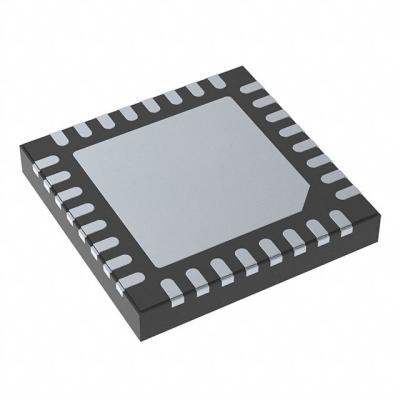
LCMXO2-2000HC-4TG144C Integrated Circuit Chip FPGA 111 I/O 144TQFP
| TYPE | DESCRIPTION |
| Category | Integrated Circuits (ICs) |
| Embedded | |
| FPGAs (Field Programmable Gate Array) | |
| Mfr | Lattice Semiconductor Corporation |
| Series | MachXO2 |
| Packaging | Tray |
| Number of LABs/CLBs | 264 |
| Number of Logic Elements/Cells | 2112 |
| Total RAM Bits | 75776 |
| Number of I/O | 111 |
| Voltage - Supply | 2.375V ~ 3.465V |
| Mounting Type | Surface Mount |
| Operating Temperature | 0°C ~ 85°C (TJ) |
| Package / Case | 144-LQFP |
| Supplier Device Package | 144-TQFP (20x20) |
| Base Product Number | LCMXO2-2000 |
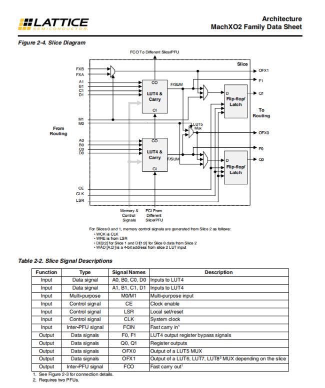
Features of LCMXO2-2000HC-4TG144C
•
On-Chip
User
Flash
Memory
•
Up
to
256
kbits
of
User
Flash
Memory
•
100,000
write
cycles
•
Accessible
through
WISHBONE,
SPI,
I2C
and
JTAG
interfaces
•
Can
be
used
as
soft
processor
PROM
or
as
Flash
memory
•
Pre-Engineered
Source
Synchronous
I/O
•
DDR
registers
in
I/O
cells
•
Dedicated
gearing
logic
•
7:1
Gearing
for
Display
I/Os
•
Generic
DDR,
DDRX2,
DDRX4
•
Dedicated
DDR/DDR2/LPDDR
memory
with
DQS
support
•
High
Performance,
Flexible
I/O
Buffer
•
Programmable
sysIO™
buffer
supports
wide
range
of
interfaces:
–
LVCMOS
3.3/2.5/1.8/1.5/1.2
–
LVTTL
–
PCI
–
LVDS,
Bus-LVDS,
MLVDS,
RSDS,
LVPECL
–
SSTL
25/18
–
HSTL
18
–
Schmitt
trigger
inputs,
up
to
0.5
V
hysteresis
•
I/Os
support
hot
socketing
•
On-chip
differential
termination
•
Programmable
pull-up
or
pull-down
mode
•
Flexible
On-Chip
Clocking
•
Eight
primary
clocks
•
Up
to
two
edge
clocks
for
high-speed
I/O
interfaces
(top
and
bottom
sides
only)
•
Up
to
two
analog
PLLs
per
device
with
fractional-n
frequency
synthesis
–
Wide
input
frequency
range
(7
MHz
to
400
MHz)
•
Non-volatile,
Infinitely
Reconfigurable
•
Instant-on
–
powers
up
in
microseconds
•
Single-chip,
secure
solution
•
Programmable
through
JTAG,
SPI
or
I2C
•
Supports
background
programming
of
non-volatile
memory
•
Optional
dual
boot
with
external
SPI
memory
•
TransFR™
Reconfiguration
•
In-field
logic
update
while
system
operates
•
Enhanced
System
Level
Support
•
On-chip
hardened
functions:
SPI,
I2C,
timer/counter
•
On-chip
oscillator
with
5.5%
accuracy
•
Unique
TraceID
for
system
tracking
•
One
Time
Programmable
(OTP)
mode
•
Single
power
supply
with
extended
operating
range
•
IEEE
Standard
1149.1
boundary
scan
•
IEEE
1532
compliant
in-system
programming
Descriptions of LCMXO2-2000HC-4TG144C
Every
device
in
the
family
has
a
JTAG
port
that
supports
programming
and
configuration
of
the
device
as
well
as
access
to
the
user
logic.
The
MachXO2
devices
are
available
for
operation
from
3.3
V,
2.5
V
and
1.2
V
power
supplies,
providing
easy
integration
into
the
overall
system.
Environmental
&
Export
Classifications
of LCMXO2-2000HC-4TG144C
| ATTRIBUTE | DESCRIPTION |
| RoHS Status | ROHS3 Compliant |
| Moisture Sensitivity Level (MSL) | 3 (168 Hours) |
| REACH Status | REACH Unaffected |
| ECCN | EAR99 |
| HTSUS | 8542.39.0001 |