

| Price | by case |
| MOQ | 5pcs |
| Delivery Time | 2-4weeks |
| Brand | zmkj |
| Place of Origin | CHINA |
| Model Number | 6inch S-C-N |
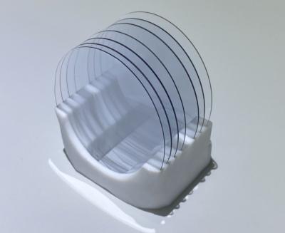
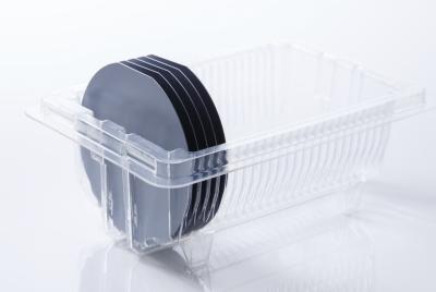
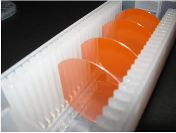
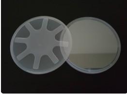
| Packaging Details | single wafer packed in 6"plastic box under N2 |
| Payment Terms | T/T, Western Union, MoneyGram |
| Supply Ability | 500pcs per month |
| Place of Origin | CHINA | thickness | 650um or customzied |
| Packaging Details | single wafer packed in 6"plastic box under N2 | SIZE | 6INCH |
| Material | GaAs single crystal | Model Number | 6inch S-C-N |
| Orientation | (100)2°off | Supply Ability | 500pcs per month |
| Surface | DSP | Brand Name | zmkj |
| Payment Terms | T/T, Western Union, MoneyGram | Growth method | VFG |
| Price | by case | Delivery Time | 2-4weeks |
| Minimum Order Quantity | 5pcs | OF type | notch or OF Flat |
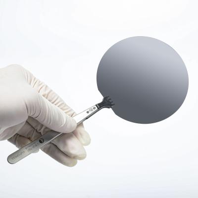
(GaAs) Gallium Arsenide Wafers
PWAM Develops and manufactures compound semiconductor substrates-gallium arsenide crystal and wafer.We has used advanced crystal growth technology,vertical gradient freeze(VGF) and GaAs wafer processing technology,established a production line from crystal growth, cutting, grinding to polishing processing and built a 100-class clean room for wafer cleaning and packaging. Our GaAs wafer include 2~6 inch ingot/wafers for LED,LD and Microelectronics applications.We are always dedicated to improve the quality of currently substates and develop large size substrates.
(GaAs)Gallium Arsenide Wafers for LED Applications

|
SPECIFICATION
--6
inch
SI-Dopant
N-Type
SSP/DSP
LED/LD
Gallium
Arsenide
wafer
|
|
|
Growth
method
|
VGF
|
|
Orientation
|
<100>
|
|
Diameter
|
150.0
+/-
0.3
mm
|
|
Thickness
|
650um
+/-
25um
|
|
Polish
|
Single
sided
polished
(SSP)
|
|
Surface
Roughness
|
Polished
|
|
TTV/Bow
|
<10um
/<10um
|
|
Dopant
|
Si
|
|
Conductivity
type
|
N-type
|
|
Resistivity(at
RT)
|
(1.2~9.9)*10-3
ohm
cm
|
|
Etch
Pit
Density(EPD)
|
LED
<5000
/cm2
;
LD
<500
/cm2
|
|
Mobility
|
LED
>1000
cm2/v.s
;
LD
>1500
cm2/v.s
|
|
Carrier
Concentration
|
LED
>(0.4-4)*1018
/cm3
;
LD
>(0.4-2.5)*1018
/cm3
|
Specifications of semi-conducting GaAs wafer
|
Growth Method |
VGF |
|||
|
Dopant |
p-type: Zn |
n-type: Si |
||
|
Wafer Shape |
Round (DIA: 2", 3", 4", 6") |
|||
|
Surface Orientation * |
(100)±0.5° |
|||
|
* Other Orientations maybe available upon request |
||||
|
Dopant |
Si (n-type) |
Zn (p-type) |
||
|
Carrier Concentration (cm-3) |
( 0.8-4) × 1018 |
( 0.5-5) × 1019 |
||
|
Mobility (cm2/V.S.) |
( 1-2.5) × 103 |
50-120 |
||
|
Etch Pitch Density (cm2) |
100-5000 |
3,000-5,000 |
||
|
Wafer Diameter (mm) |
50.8±0.3 |
76.2±0.3 |
100±0.3 |
|
|
Thickness (µm) |
350±25 |
625±25 |
625±25 |
|
|
TTV [P/P] (µm) |
≤ 4 |
≤ 4 |
≤ 4 |
|
|
TTV [P/E] (µm) |
≤ 10 |
≤ 10 |
≤ 10 |
|
|
WARP (µm) |
≤ 10 |
≤ 10 |
≤ 10 |
|
|
OF (mm) |
17±1 |
22±1 |
32.5±1 |
|
|
OF / IF (mm) |
7±1 |
12±1 |
18±1 |
|
|
Polish* |
E/E, P/E, P/P |
E/E, P/E, P/P |
E/E, P/E, P/P |
|
Specifications of semi-insulating GaAs wafer
|
Growth Method |
VGF |
|||
|
Dopant |
SI Type: Carbon |
|||
|
Wafer Shape |
Round (DIA: 2", 3", 4", 6") |
|||
|
Surface Orientation * |
(100)±0.5° |
|||
|
* Other Orientations maybe available upon request |
||||
|
Resistivity (Ω.cm) |
≥ 1 × 10⁷ |
≥ 1 × 10⁸ |
||
|
Mobility (cm2/V.S) |
≥ 5,000 |
≥ 4,000 |
||
|
Etch Pitch Density (cm2) |
1,500-5,000 |
1,500-5,000 |
||
|
Wafer Diameter (mm) |
50.8±0.3 |
76.2±0.3 |
100±0.3 |
150±0.3 |
|
Thickness (µm) |
350±25 |
625±25 |
625±25 |
675±25 |
|
TTV [P/P] (µm) |
≤ 4 |
≤ 4 |
≤ 4 |
≤ 4 |
|
TTV [P/E] (µm) |
≤ 10 |
≤ 10 |
≤ 10 |
≤ 10 |
|
WARP (µm) |
≤ 10 |
≤ 10 |
≤ 10 |
≤ 15 |
|
OF (mm) |
17±1 |
22±1 |
32.5±1 |
NOTCH |
|
OF / IF (mm) |
7±1 |
12±1 |
18±1 |
N/A |
|
Polish* |
E/E, P/E, P/P |
E/E, P/E, P/P |
E/E, P/E, P/P |
E/E, P/E, P/P |

FAQ
–
Q:
What
you
can
supply
logistics
and
cost?
(1)
We
accept
DHL,
Fedex,
TNT,
UPS,
EMS,
SF
and
etc.
(2)
If
you
have
your
own
express
number,
it's
great.
If
not,
we
could
assist
you
to
deliver.
Freight=USD25.0(the
first
weight)
+
USD12.0/kg
Q:
What's
the
delivery
time?
(1)
For
the
standard
products
such
as
ball
lens,
powell
lens
and
collimator
lens:
For
inventory:
the
delivery
is
5
workdays
after
order.
For
customized
products:
the
delivery
is
2
or
3
workweeks
after
order.
(2)
For
the
off-standard
products,
the
delivery
is
2
or
6
workweeks
after
you
place
the
order.
Q:
How
to
pay?
T/T,
Paypal,
West
Union,
MoneyGram,
Secure
payment
and
Trade
Assurance
on
Alibaba
and
etc..
Q:
What's
the
MOQ?
(1)
For
inventory,
the
MOQ
is
5pcs.
(2)
For
customized
products,
the
MOQ
is
5pcs-20pcs.
It
depends
on
quantity
and
technics
Q:
Do
you
have
inspection
report
for
material?
We
can
supply
detail
report
for
our
products.
Packaging
–
Logistcs
we
concern each
details
of
the
package
,
cleaning,
anti-static
,
shock
treatment
.
According
to
the
quantity
and
shape
of
the
product
,
we will take a different packaging process!