

| Price | by case |
| MOQ | 5pcs |
| Delivery Time | 2-4weeks |
| Brand | zmkj |
| Place of Origin | CHINA |
| Model Number | 4inch SEMI |
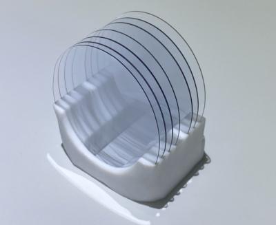
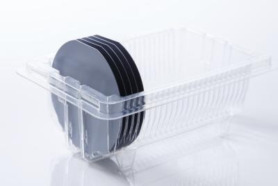
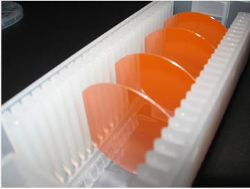
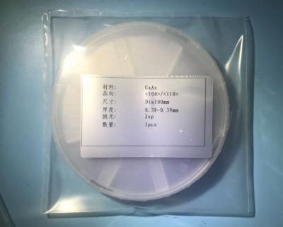
| Packaging Details | single wafer packed in 6"plastic box under N2 |
| Payment Terms | T/T, Western Union, MoneyGram |
| Supply Ability | 500pcs per month |
| Place of Origin | CHINA | thickness | 625um or customzied |
| Packaging Details | single wafer packed in 6"plastic box under N2 | SIZE | 4INCH |
| Material | GaAs single crystal | Model Number | 4inch SEMI |
| Orientation | (100)2°off | Supply Ability | 500pcs per month |
| Surface | DSP | Brand Name | zmkj |
| Payment Terms | T/T, Western Union, MoneyGram | Growth method | VFG |
| Price | by case | Delivery Time | 2-4weeks |
| Minimum Order Quantity | 5pcs | OF type | OF Flat |
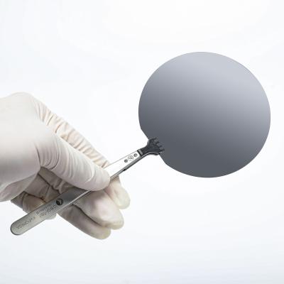
Our 2’’ to 6’’ semi-conducting & semi-insulating GaAs crystal & wafer are wildly used in semiconductor integrated circuit application & LED general lighting application.
| Feature | Application field |
|---|---|
| High electron mobility | Light emitting diodes |
| High frequency | Laser diodes |
| High conversion efficiency | Photovoltaic devices |
| Low power consumption | High Electron Mobility Transistor |
| Direct band gap | Heterojunction Bipolar Transistor |


Specifications of semi-conducting GaAs wafer
|
Growth Method |
VGF |
|||
|
Dopant |
p-type: Zn |
n-type: Si |
||
|
Wafer Shape |
Round (dia: 2", 3", 4", 6") |
|||
|
Surface Orientation * |
(100)±0.5° |
|||
|
* Other Orientations maybe available upon request |
||||
|
Dopant |
Si (n-type) |
Zn (p-type) |
||
|
Carrier Concentration (cm-3) |
( 0.8-4) × 1018 |
( 0.5-5) × 1019 |
||
|
Mobility (cm2/V.S.) |
( 1-2.5) × 103 |
50-120 |
||
|
Etch Pitch Density (cm2) |
100-5000 |
3,000-5,000 |
||
|
Wafer Diameter (mm) |
50.8±0.3 |
76.2±0.3 |
100±0.3 |
|
|
Thickness (µm) |
350±25 |
625±25 |
625±25 |
|
|
TTV [P/P] (µm) |
≤ 4 |
≤ 4 |
≤ 4 |
|
|
TTV [P/E] (µm) |
≤ 10 |
≤ 10 |
≤ 10 |
|
|
WARP (µm) |
≤ 10 |
≤ 10 |
≤ 10 |
|
|
OF (mm) |
17±1 |
22±1 |
32.5±1 |
|
|
OF / IF (mm) |
7±1 |
12±1 |
18±1 |
|
|
Polish* |
E/E, |
E/E, |
E/E, |
|
Specifications of semi-insulating GaAs wafer
|
Growth Method |
VGF |
|||
|
Dopant |
SI Type: Carbon |
|||
|
Wafer Shape |
Round (DIA: 2", 3", 4", 6") |
|||
|
Surface Orientation * |
(100)±0.5° |
|||
|
* Other Orientations maybe available upon request |
||||
|
Resistivity (Ω.cm) |
≥ 1 × 10⁷ |
≥ 1 × 10⁸ |
||
|
Mobility (cm2/V.S) |
≥ 5,000 |
≥ 4,000 |
||
|
Etch Pitch Density (cm2) |
1,500-5,000 |
1,500-5,000 |
||
|
Wafer Diameter (mm) |
50.8±0.3 |
76.2±0.3 |
100±0.3 |
150±0.3 |
|
Thickness (µm) |
350±25 |
625±25 |
625±25 |
675±25 |
|
TTV [P/P] (µm) |
≤ 4 |
≤ 4 |
≤ 4 |
≤ 4 |
|
TTV [P/E] (µm) |
≤ 10 |
≤ 10 |
≤ 10 |
≤ 10 |
|
WARP (µm) |
≤ 10 |
≤ 10 |
≤ 10 |
≤ 15 |
|
OF (mm) |
17±1 |
22±1 |
32.5±1 |
NOTCH |
|
OF / IF (mm) |
7±1 |
12±1 |
18±1 |
N/A |
|
Polish* |
E/E, |
E/E, |
E/E, |
E/E, |


FAQ
–
Q:
What
you
can
supply
logistics
and
cost?
(1)
We
accept
DHL,
Fedex,
TNT,
UPS,
EMS,
SF
and
etc.
(2)
If
you
have
your
own
express
number,
it's
great.
If
not,
we
could
assist
you
to
deliver.
Freight=USD25.0(the
first
weight)
+
USD12.0/kg
Q:
How
to
pay?
T/T,
Paypal,
West
Union,
MoneyGram,
Secure
payment
and
Trade
Assurance
on
Alibaba
and
etc..
Q:
What's
the
MOQ?
(1)
For
inventory,
the
MOQ
is
5pcs.
(2)
For
customized
products,
the
MOQ
is
5pcs-20pcs.
It
depends
on
quantity
and
technics
Q:
Do
you
have
inspection
report
for
material?
We
can
supply
detail
report
for
our
products.
Packaging
–
Logistcs
we
concern
each
details
of
the
package
,
cleaning,
anti-static
,
shock
treatment
.
According
to
the
quantity
and
shape
of
the
product
,
we
will
take
a
different
packaging
process!