Impedance
Controlled
PCB
Differential
Impedance
Circuit
Board
8
Layer
PCB
for
Wireless
HDMI
1.1
General
description
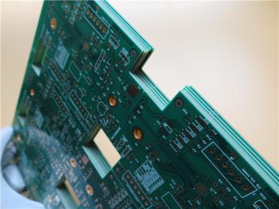
This
is
a
type
of
8
layer
printed
circuit
board
built
on
FR-4
substrate
with
Tg
170°C
for
the
application
of
Wireless
HDMI.
It's
1.6
mm
thick
with
white
silkscreen(Taiyo)
on
green
solder
mask
(Taiyo)
and
immersion
gold
on
pads.
It's
also
an
impedance
controlled
PCB
with
single-end
impedance
and
differential
impedance
controlled
on
on
top
layer
and
bottom
layer.
The
base
material
is
from
Taiwan
ITEQ
supplying
1
up
PCB
per
panel.
They're
fabricated
per
IPC
6012
Class
2
using
supplied
Gerber
data.
Each
25
panels
are
packed
for
shipment.
1.2
Features
and
benifits
Lead
free
assemblies
with
a
maximum
reflow
temperature
of
260℃
High
solderability,
no
stressing
of
circuit
boards
and
less
contamination
of
PCB
surface.
AOI
inspection
8000
types
of
PCB
per
month
12
hours
quotation
Free-of-charge
PCB
panelization
1.3
Applications
USB
Adapter
WiFi
USB
Dongle
GPRS
Modem
1.4
Parameter
and
data
sheet
|
PCB
SIZE
|
109.3
x
107.41mm=1PCS
|
|
BOARD
TYPE
|
Multilayer
PCB
|
|
Number
of
Layers
|
8
layers
|
|
Surface
Mount
Components
|
YES
|
|
Through
Hole
Components
|
YES
|
|
LAYER
STACKUP
|
copper
-------
18um(0.5oz)+plate
TOP
layer
|
|
Prepreg
7628(43%)
0.195mm
|
|
copper
-------
35um(1oz)
MidLayer
1
|
|
FR-4
0.2mm
|
|
copper
-------
35um(1oz)
MidLayer
2
|
|
Prepreg
7628(43%)
0.195mm
|
|
copper
-------
35um(1oz)
MidLayer
3
|
|
FR-4
0.2mm
|
|
copper
-------
35um(1oz)
MidLayer
4
|
|
Prepreg
7628(43%)
0.195mm
|
|
copper
-------
35um(1oz)
MidLayer
5
|
|
FR-4
0.2mm
|
|
copper
-------
35um(1oz)
MidLayer
6
|
|
Prepreg
7628(43%)
0.195mm
|
|
copper
-------
18um(0.5oz)+plate
BOT
Layer
|
|
TECHNOLOGY
|
|
|
Minimum
Trace
and
Space:
|
4mil/4mil
|
|
Minimum
/
Maximum
Holes:
|
0.3/6.19mm
|
|
Number
of
Different
Holes:
|
24
|
|
Number
of
Drill
Holes:
|
5158
|
|
Number
of
Milled
Slots:
|
0
|
|
Number
of
Internal
Cutouts:
|
0
|
|
Impedance
Control:
|
Single-Ended
Trace
Width:L1,
L3,
L6,
L8
4mils
---
50
ohm,
Differential
trace/space:
top
layer
5.1/6.0
mils
--
90
ohm,
5.1
/
8
mils
---
100
ohm,
L6
5.1
/
8
mils
---
100
ohm;
bottom
layer
5.1
mil
/6
mils
---
90
ohm,
5.1mils
/
8
mils
---
100
ohm
|
|
Number
of
Gold
finger:
|
0
|
|
BOARD
MATERIAL
|
|
|
Glass
Epoxy:
|
FR-4
TG170℃,
er<5.4.IT-180,
ITEQ
Supplied
|
|
Final
foil
external:
|
1oz
|
|
Final
foil
internal:
|
1oz
|
|
Final
height
of
PCB:
|
1.6mm
±0.16
|
|
PLATING
AND
COATING
|
|
|
Surface
Finish
|
Immersion
gold
(26.1%
)
0.05µm
over
3µm
nickel
|
|
Solder
Mask
Apply
To:
|
TOP
and
Bottom,
12micron
Minimum
|
|
Solder
Mask
Color:
|
Green,
PSR-2000GT600D,
Taiyo
Supplied.
|
|
Solder
Mask
Type:
|
LPSM
|
|
CONTOUR/CUTTING
|
Routing,
stamp
holes.
|
|
MARKING
|
|
|
Side
of
Component
Legend
|
TOP
and
Bottom.
|
|
Colour
of
Component
Legend
|
White,
IJR-4000
MW300,
Taiyo
Supplied.
|
|
Manufacturer
Name
or
Logo:
|
Marked
on
the
board
in
a
conductor
and
leged
FREE
AREA
|
|
VIA
|
Plated
through
hole(PTH),
Via
in
pad,
Resin
via
plug,
via
capped.
|
|
FLAMIBILITY
RATING
|
UL
94-V0
Approval
MIN.
|
|
DIMENSION
TOLERANCE
|
|
|
Outline
dimension:
|
0.0059"
(0.15mm)
|
|
Board
plating:
|
0.0030"
(0.076mm)
|
|
Drill
tolerance:
|
0.002"
(0.05mm)
|
|
TEST
|
100%
Electrical
Test
prior
shipment
|
|
TYPE
OF
ARTWORK
TO
BE
SUPPLIED
|
email
file,
Gerber
RS-274-X,
PCBDOC
etc
|
|
SERVICE
AREA
|
Worldwide,
Globally.
|
1.5
Characteristic
Impedance
The
characteristic
impedance
of
the
conductor
on
the
printed
circuit
board
is
an
important
indicator
of
the
circuit
design,
especially
in
the
PCB
design
of
high
frequency
circuit.
Whether
the
characteristic
impedance
of
the
conductor
is
consistent
and
matching
with
the
characteristic
impedance
required
by
the
device
or
signal
must
be
taken
into
consideration.
Therefore,
these
two
concepts
in
reliability
design
of
PCB
design
must
be
paid
attention.
There
will
be
a
variety
of
signal
transmission
in
the
conductor
of
circuit
board.
To
increase
the
rate
of
transmission,
it
must
increase
its
frequency.
Due
to
the
factors
of
the
circuit
itself
such
as
etching,
stack
thickness,
track
width
and
so
on
are
different,
it
will
cause
changes
of
the
impedance
value,
resulting
in
its
signal
distortion.
Therefore,
the
impedance
value
of
conductor
on
high-speed
circuit
board
should
be
controlled
within
a
certain
range,
known
as
the
"impedance
control".
The
factors
that
affect
the
impedance
of
the
PCB
wiring
are
mainly
the
width
of
the
copper
track,
the
thickness
of
the
copper
track,
the
dielectric
constant
of
the
dielectric,
the
thickness
of
the
dielectric,
the
thickness
of
the
pad,
the
path
of
the
ground
layer,
the
wires
around
the
wiring,
etc.
So
the
impedance
of
the
wiring
on
the
board
must
be
controlled
in
the
design
of
the
PCB
to
avoid
signal
reflection
and
other
electromagnetic
interference
and
signal
integrity
issues
as
far
as
possible,
to
guarantee
the
stability
of
the
actual
use
of
the
PCB
board.
You
can
refer
to
the
corresponding
empirical
formula
for
the
calculation
method
of
micro-strip
line
and
strip
line
impedance
on
PCB
board.
![]()