Differential
Impedance
Controlled
PCB
Single-End
Impedance
Circuit
Board
10
Layer
PCB
Board
Satellite
systems
1.1
General
description
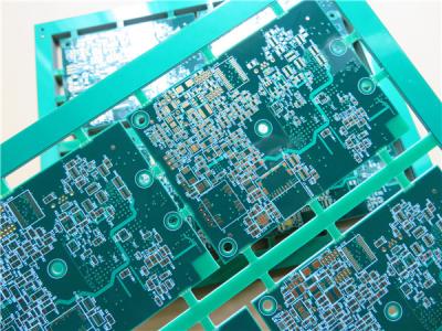
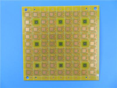
This
is
a
type
of
multilayer
PCB
built
on
FR-4
substrate
with
Tg
170°C
for
the
application
of
Satellite
systems
with
10
layer
copper.
It's
1.6
mm
thick
with
white
silkscreen(Taiyo)
on
green
solder
mask
(Taiyo)
and
immersion
gold
on
pads.
This
is
also
an
impedance
controlled
PCB
with
50
ohm
single-end
impedance
and
97
ohm
with
differential
impedance
control.
The
base
material
is
from
ITEQ
supplying
4
up
PCBs
per
panel.
They're
fabricated
per
IPC
6012
Class
2
using
supplied
Gerber
data.
Each
25
panels
are
packed
for
shipment.
1.2
Features
and
benifits
Lead
free
assemblies
with
a
maximum
reflow
temperature
of
260℃
SMT
process
is
resistant
to
reflow
soldering,
resistant
to
rework.
The
signal
lines
form
a
constant
low
impedance
to
the
ground
Strict
WIP
inspection
and
monitoring
as
well
as
working
instruction
UL,
ISO14001,
TS16949
certified
Hassle-free,
one-to-one
after-sales
service
Delivery
on
time:
>98%
1.3
Applications
GPS
Tracking
Devices
GSM
Signal
Booster
Automotive
dashboards
1.4
Parameter
and
data
sheet
|
PCB
SIZE
|
199
x
170mm=4PCS
|
|
BOARD
TYPE
|
Multilayer
PCB
|
|
Number
of
Layers
|
10
layers
|
|
Surface
Mount
Components
|
YES
|
|
Through
Hole
Components
|
YES
|
|
LAYER
STACKUP
|
copper
-------
18um(0.5oz)+plate
TOP
layer
|
|
Prepreg
0.1016mm
(4mil)
|
|
copper
-------
35um(1oz)
Plane
GND
|
|
FR-4
0.127mm
(5
mil)
|
|
copper
-------
18um(0.5
oz)
Signal
SIG1
|
|
Prepreg
0.127
mm
(5mil)
|
|
copper
-------
18um(0.5
oz)
Signal
SIG2
|
|
Prepreg
0.127mm
(5
mil)
|
|
copper
-------
35um(1oz)
Plane
PWR
|
|
FR-4
0.330mm
(13mil)
|
|
copper
-------
35um(1oz)
Plane
GND
|
|
Prepreg
0.127mm
(5
mil)
|
|
copper
-------
18
um(0.5
oz)
Signal
SIG3
|
|
Prepreg
0.127mm
(5
mil)
|
|
copper
-------
18
um(0.5
oz)
Signal
SIG4
|
|
Prepreg
0.127mm
(5
mil)
|
|
copper
-------
35um(1oz)
Plane
GND
|
|
Prepreg
0.1016mm
(4mil)
|
|
copper
-------
35um(1oz)
Signal
BOT
|
|
TECHNOLOGY
|
|
|
Minimum
Trace
and
Space:
|
4mil/4mil
|
|
Minimum
/
Maximum
Holes:
|
0.25/4.2mm
|
|
Number
of
Different
Holes:
|
15
|
|
Number
of
Drill
Holes:
|
850
|
|
Number
of
Milled
Slots:
|
10
|
|
Number
of
Internal
Cutouts:
|
0
|
|
Impedance
Control:
|
YES.
Top
layer,
7.0
mil
trace
50
ohms
single
end.
Layer
3
signal
layer,
4.0/4.0
mil
trace-space
differential
impedance
=
91
ohms;
4.0/6.0
mil
trace-space
differential
impedance
=
97
ohms.
|
|
Number
of
Gold
finger:
|
0
|
|
BOARD
MATERIAL
|
|
|
Glass
Epoxy:
|
FR-4
TG170℃,
er<5.4.IT-180,
ITEQ
Supplied
|
|
Final
foil
external:
|
1oz
|
|
Final
foil
internal:
|
1oz
|
|
Final
height
of
PCB:
|
1.6mm
±0.16
|
|
PLATING
AND
COATING
|
|
|
Surface
Finish
|
Immersion
gold
(30.1%
)
0.1µm
over
3µm
nickel
|
|
Solder
Mask
Apply
To:
|
TOP
and
Bottom,
12micron
Minimum
|
|
Solder
Mask
Color:
|
Green,
PSR-2000
KX700G,
Taiyo
Supplied.
|
|
Solder
Mask
Type:
|
LPSM
|
|
CONTOUR/CUTTING
|
Routing,
stamp
holes.
|
|
MARKING
|
|
|
Side
of
Component
Legend
|
TOP
and
Bottom.
|
|
Colour
of
Component
Legend
|
White,
S-380W,
Taiyo
Supplied.
|
|
Manufacturer
Name
or
Logo:
|
Marked
on
the
board
in
a
conductor
and
leged
FREE
AREA
|
|
VIA
|
plated
through
hole(PTH),
minimum
via
10
mils.
|
|
FLAMIBILITY
RATING
|
UL
94-V0
Approval
MIN.
|
|
DIMENSION
TOLERANCE
|
|
|
Outline
dimension:
|
0.0059"
|
|
Board
plating:
|
0.0029"
|
|
Drill
tolerance:
|
0.002"
|
|
TEST
|
100%
Electrical
Test
prior
shipment
|
|
TYPE
OF
ARTWORK
TO
BE
SUPPLIED
|
email
file,
Gerber
RS-274-X,
PCBDOC
etc
|
|
SERVICE
AREA
|
Worldwide,
Globally.
|
![]()
1.5
Impedance
PCB-
Impedance
match
If
there
is
signal
transmission
in
the
circuit
board,
it
is
expected
to
be
smoothly
transmitted
from
the
sending
end
to
the
receiving
end
under
the
condition
of
minimum
energy
loss,
and
the
receiving
end
can
completely
absorbs
it
without
any
reflection.
To
achieve
this
kind
of
transmission,
the
impedance
of
the
circuit
must
be
equal
to
the
internal
impedance
of
the
sending
end,
which
is
called
"impedance
match."
So
when
the
signal
is
transmitted
in
the
PCB,
the
characteristic
impedance
of
the
PCB
board
must
be
matched
with
the
electronic
impedance
of
the
head
and
tail
components.
Once
the
impedance
value
exceeds
the
tolerance,
the
transmitted
signal
energy
will
be
reflected,
scattered,
attenuated
or
delayed,
resulting
in
incomplete
signal
and
signal
distortion.
Impedance
match
is
one
of
the
design
elements
when
designing
high-speed
PCB
circuits.
However,
the
impedance
value
is
absolutely
related
with
wiring
mode.
For
example,
whether
wiring
on
the
surface
layer
or
inner
layer,
the
distance
from
the
reference
power
layer
or
ground
layer,
the
width
of
wiring,
the
PCB
material,
etc.
will
affect
the
characteristic
impedance
of
wiring.
That
is
to
say,
the
impedance
value
can
be
determined
only
after
wiring
layout,
while
the
characteristic
impedance
produced
by
different
PCB
manufacturers
is
also
slightly
different.
The
wiring
layout
condition
of
impedance
discontinuity
cannot
be
completely
considered
in
general
simulation
software
due
to
the
limitation
of
the
circuit
model
or
the
mathematical
algorithm
used.
In
this
case,
only
some
temninators,
such
as
series
resistors,
can
be
reserved
on
the
schematic
diagram
to
mitigate
the
effect
of
discontinuous
wiring
impedance.
The
method
to
completely
solve
the
problem
is
still
trying
to
avoid
the
occurrence
of
impedance
discontinuities
when
wiring
layout.
![]()