| Price | Please make an enquiry |
| MOQ | 1000PCS |
| Delivery Time | 3-4 weeks |
| Brand | ESEN |
| Place of Origin | Shenzhen China |
| Certification | ISO9001/ISO14001 |
| Model Number | HP12832-65-TSWG4P091 |
| Packaging Details | All the products are packed in right way |
| Payment Terms | T/T,L/C |
| Supply Ability | 300K/mth |
| Thinner version OLED | Suitable for Wearable Device | Place of Origin | Shenzhen China |
| Size | 0.91 inch | Packaging Details | All the products are packed in right way |
| Pixel Size | 0.152 x 0.152mm | Dot Matrix | 128 x 32 Dots |
| Display Mode | Passive Matrix | Model Number | HP12832-65-TSWG4P091 |
| Supply Ability | 300K/mth | Certification | ISO9001/ISO14001 |
| Module dimension | 30.0 x11.5 x1.26mm | Display Color | White / Yellow / Sky Blue |
| Brand Name | ESEN | Payment Terms | T/T,L/C |
| Pixel Pitch | 0.175 x0.175mm | Type | Graphic |
| Price | Please make an enquiry | Delivery Time | 3-4 weeks |
| Minimum Order Quantity | 1000PCS | Active Area | 22.384 x5.584 mm |
| IC | SSD1306BZ | Structure | COG |
| Interface | l2C OLED Display/ OLED Display 12C | Drive Duty | 1/32 Duty |
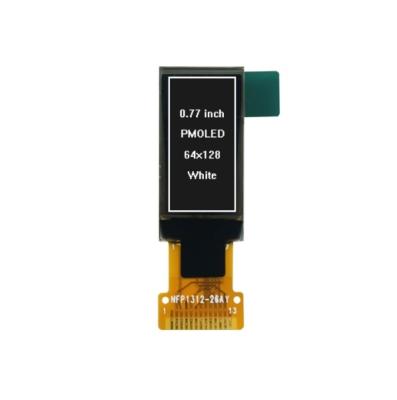
| Size | 0.91 inch |
| Dot Matrix | 128 x 32 Dots |
| Module dimension | 30.0 x 11.5 x 1.26mm |
| Active Area | 22.384 x 5.584 mm |
| Pixel Size | 0.152 x 0.152mm |
| Pixel Pitch | 0.175 x 0.175mm |
| Display Mode | Passive Matrix |
| Display Color | White / Yellow / Sky Blue |
| Drive Duty | 1/32 Duty |
| IC | SSD1306BZ |
| Interface | I2C OLED Display |
| Type | Graphic |
| Structure | COG |
| Special Feature | Thinner version OLED - Suitable for Wearable Device |
Winstar HP12832-65-TSWG4P091 is a popular small OLED display which is made of 128x32 pixels, diagonal size 0.91 inch, making it very suitable for wearable devices. The module is built with SSD1306 controller IC and supports I2C interface with 14 pins FPC pinout.
This COG structure I2C OLED display has a built-in controller with voltage generation requiring only a single 3V power supply. The display module is lightweight, low power and small, making it suitable for wall/meter devices, home applications, Cloud/IoT systems, handheld instruments, intelligent technology devices, energy systems, automotive, communication systems, medical instruments, and wearable devices.
The module can operate at temperatures from -40℃ to +80℃ with storage temperatures ranging from -40℃ to +85℃.

| Parameter | Symbol | Min | Max | Unit |
|---|---|---|---|---|
| Supply Voltage for Logic | VDD | 0 | 4.0 | V |
| Supply Voltage for Display | VCC | 0 | 16.0 | V |
| Operating Temperature | TOP | -40 | +80 | °C |
| Storage Temperature | TSTG | -40 | +85 | °C |
| Item | Symbol | Condition | Min | Typ | Max | Unit |
|---|---|---|---|---|---|---|
| Supply Voltage for Logic | VDD | - | 2.8 | 3.0 | 3.3 | V |
| Supply Voltage for Display | VCC | - | 7 | 7.25 | 8 | V |
| Input High Volt. | VIH | - | 0.8×VDD | - | VDDIO | V |
| Input Low Volt. | VIL | - | 0 | - | 0.2×VDD | V |
| No. | Symbol | Function |
|---|---|---|
| 1 | C2P | Positive Terminal of the Flying Inverting CapacitorNegative Terminal of the Flying Boost CapacitorThe charge-pump capacitors are required between the terminals. They must be floated when the converter is not used. |
| 2 | C2N | |
| 3 | C1P | |
| 4 | C1N | |
| 5 | VBAT | Power Supply for DC/DC Converter Circuit. This is the power supply pin for the internal buffer of the DC/DC voltage converter. It must be connected to external source when the converter is used. It should be connected to VDD when the converter is not used. |
| 6 | NC | No connection |
| 7 | VSS | Ground of Logic Circuit. This is a ground pin. It acts as a reference for the logic pins. It must be connected to external ground. |
| 8 | VDD | Power Supply for Logic. This is a voltage supply pin. It must be connected to external source. |
| 9 | RES# | Power Reset for Controller and Driver. This pin is reset signal input. When the pin is low, initialization of the chip is executed. |
| 10 | SCL | I2C mode is selected, D2, D1 should be tied together and serve as SDAout, SDAin in application and D0 is the serial clock input, SCL. |
| 11 | SDA | |
| 12 | IREF | Current Reference for Brightness Adjustment. This pin is segment current reference pin. A resistor should be connected between this pin and VSS. Set the current lower than 12.5μA. |
| 13 | VCOMH | Voltage Output High Level for COM Signal. This pin is the input pin for the voltage output high level for COM signals. A capacitor should be connected between this pin and VSS. |
| 14 | VCC | Power Supply for OEL Panel. This is the most positive voltage supply pin of the chip. A stabilization capacitor should be connected between this pin and VSS when the converter is used. It must be connected to external source when the converter is not used. |