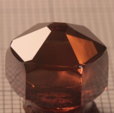
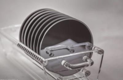
30mm Dia AlN Single Crystal Semiconductor Substrate
Price: by case
MOQ: 3pcs
Delivery Time: in 30days
Brand: ZMKJ
View More
diameter 150mm 8inch 4inch 6inch Silicon-based AlN templates 500nm AlN film on silicon substrate Applications of AlN template Silicon-based semiconductor technology has reached its limits and could not satisfy the requirements of future electronic devices. As a typical kind of 3rd/4th-generation sem... View More
{"cid":"40149","pid":"14102882","pimg_url":"\/\/img1.ecerimg.com\/c9\/fb\/2e8a38b9eeeb\/product\/35041874_s-w400xh400.jpg","name":"30mm Dia AlN Single Crystal Semiconductor Substrate","inquiry_url":"\/corp\/inquiry-new\/uu4zrn-udj4x2.html","attrs":{"Price":"by case","MOQ":"3pcs","Delivery Time":"in 30days","Brand":"ZMKJ"}}
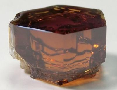
5G Saw Diameter 10mm Single Crystal AlN Semiconductor Substrate
Price: by case
MOQ: 1pcs
Delivery Time: in 30days
Brand: ZMKJ
View More
10x10mm or diameter 10mm dia25.4mm dia30mm, dia45mm, dia50.8mm AlN substrate AlN single crystal wafers Applications of AlN template Silicon-based semiconductor technology has reached its limits and could not satisfy the requirements of future electronic devices. As a typical kind of 3rd/4th-generati... View More
{"cid":"40149","pid":"14103185","pimg_url":"\/\/img1.ecerimg.com\/c9\/fb\/2e8a38b9eeeb\/product\/35043449_s-w400xh400.jpg","name":"5G Saw Diameter 10mm Single Crystal AlN Semiconductor Substrate","inquiry_url":"\/corp\/inquiry-new\/uu4zrn-udj56h.html","attrs":{"Price":"by case","MOQ":"1pcs","Delivery Time":"in 30days","Brand":"ZMKJ"}}
BAW Devices Dia 50.8mm 1 Inch AlN Aluminum Nitride Wafer
Price: by case
MOQ: 1pcs
Delivery Time: in 30days
Brand: ZMKJ
View More
dia50.8mm 2inch 1inch AlN substrate/AlN single crystal wafers 10x10mm or diameter 10mm dia25.4mm dia30mm, dia45mm, dia50.8mm AlN substrate AlN single crystal wafers Applications of AlN template we have developed a serials of proprietary processes and technologies to fabricate high-quality AlN templa... View More
{"cid":"40149","pid":"14103196","pimg_url":"\/\/img1.ecerimg.com\/c9\/fb\/2e8a38b9eeeb\/product\/35050063_s-w400xh400.jpg","name":"BAW Devices Dia 50.8mm 1 Inch AlN Aluminum Nitride Wafer","inquiry_url":"\/corp\/inquiry-new\/uu4zrn-udj56w.html","attrs":{"Price":"by case","MOQ":"1pcs","Delivery Time":"in 30days","Brand":"ZMKJ"}}
4 Inch N Type 15° Semiconductor Substrate Si Doped GaAs Wafer SSP
Price: 100-200usd/pcs
MOQ: 5pcs
Delivery Time: 2-4weeks
Brand: zmkj
View More
VFG metod N-type 2inch/3inch,4inch ,6inch dia150mm GaAs Gallium Arsenide Wafers N-type Semi-insulating type for Microelectronics, --------------------------------------------------------------------------------------------------------------(GaAs) Gallium Arsenide WafersGallium arsenide (GaAs) is a c... View More
{"cid":"40149","pid":"14104873","pimg_url":"\/\/img1.ecerimg.com\/c9\/fb\/2e8a38b9eeeb\/product\/35050305_s-w400xh400.jpg","name":"4 Inch N Type 15\u00b0 Semiconductor Substrate Si Doped GaAs Wafer SSP","inquiry_url":"\/corp\/inquiry-new\/uu4zrn-udj6v9.html","attrs":{"Price":"100-200usd\/pcs","MOQ":"5pcs","Delivery Time":"2-4weeks","Brand":"zmkj"}}
2 Inch Sapphire Substrate AlN Template Layer Wafer For 5G BAW Devices
Price: by case
MOQ: 5pcs
Delivery Time: in 30days
Brand: ZMKJ
View More
2inch 4iinch 6Inch Sapphire based AlN templates AlN film on sapphire substrate 2inch on sapphire substrate AlN Template layer Wafer For 5G BAW Devices Applications of AlN template Our OEM has developed a serials of proprietary technologies and the-state-of-the art PVT growth reactors and facilities ... View More
{"cid":"40149","pid":"14105303","pimg_url":"\/\/img1.ecerimg.com\/c9\/fb\/2e8a38b9eeeb\/product\/35052335_s-w400xh400.jpg","name":"2 Inch Sapphire Substrate AlN Template Layer Wafer For 5G BAW Devices","inquiry_url":"\/corp\/inquiry-new\/uu4zrn-udj78q.html","attrs":{"Price":"by case","MOQ":"5pcs","Delivery Time":"in 30days","Brand":"ZMKJ"}}
2'' N Semi Semiconductor Substrate Si Dopant Gallium Arsenide GaAs DSP/SSP Wafer LD/LED
Price: 100-200usd/pcs
MOQ: 5pcs
Delivery Time: 2-4weeks
Brand: zmkj
View More
VFG metod N-type 2inch/3inch,4inch ,6inch dia150mm GaAs Gallium Arsenide Wafers N-type Semi-insulating type for Microelectronics, --------------------------------------------------------------------------------------------------------------(GaAs) Gallium Arsenide WafersGallium arsenide (GaAs) is a c... View More
{"cid":"40149","pid":"11504505","pimg_url":"\/\/img1.ecerimg.com\/c9\/fb\/2e8a38b9eeeb\/product\/22723361_s-w400xh400.jpg","name":"2'' N Semi Semiconductor Substrate Si Dopant Gallium Arsenide GaAs DSP\/SSP Wafer LD\/LED","inquiry_url":"\/corp\/inquiry-new\/uu4zrn-ub2vds.html","attrs":{"Price":"100-200usd\/pcs","MOQ":"5pcs","Delivery Time":"2-4weeks","Brand":"zmkj"}}
3 Inch InP Crystal Dummy Prime Semiconductor Substrate
Price: by case
MOQ: 3pcs
Delivery Time: 2weeks
Brand: zmkj
View More
2inch InP wafers 3inch 4inch N/P TYPE InP Semiconductor Substrate Wafers Doped S+/ Zn+ /Fe + growth (modified VFG method) is used to pull a single crystal through a boric oxide liquid encapsulant starting from a seed. The dopant (Fe, S, Sn or Zn)is added to the crucible along with the polycrystal. H... View More
{"cid":"40149","pid":"13466517","pimg_url":"\/\/img1.ecerimg.com\/c9\/fb\/2e8a38b9eeeb\/product\/32220041_s-w400xh400.jpg","name":"3 Inch InP Crystal Dummy Prime Semiconductor Substrate","inquiry_url":"\/corp\/inquiry-new\/uu4zrn-ucyqen.html","attrs":{"Price":"by case","MOQ":"3pcs","Delivery Time":"2weeks","Brand":"zmkj"}}
Thick 650um 4 Inch Single Crystal InP Semiconductor Substrate
Price: by case
MOQ: 3pcs
Delivery Time: 2-4weeks
Brand: zmkj
View More
2inch InP wafers 3inch 4inch N/P TYPE InP Semiconductor Substrate Wafers Doped S+/ Zn+ /Fe + growth (modified VFG method) is used to pull a single crystal through a boric oxide liquid encapsulant starting from a seed. The dopant (Fe, S, Sn or Zn)is added to the crucible along with the polycrystal. H... View More
{"cid":"40149","pid":"13231733","pimg_url":"\/\/img1.ecerimg.com\/c9\/fb\/2e8a38b9eeeb\/product\/31169014_s-w400xh400.jpg","name":"Thick 650um 4 Inch Single Crystal InP Semiconductor Substrate","inquiry_url":"\/corp\/inquiry-new\/uu4zrn-ucqj5n.html","attrs":{"Price":"by case","MOQ":"3pcs","Delivery Time":"2-4weeks","Brand":"zmkj"}}
2-4inch N/P TYPE Semiconductor Substrate InAs Monocrystalline Crystal Substrates Wafers
Price: by case
MOQ: 3pcs
Delivery Time: 2-4weeks
Brand: zmkj
View More
2-4inch Gallium antimonide GaSb Substrate Single Crystal Monocrystal for Semiconductor InAsSb/In-AsPSb, InNAsSb and other heterojunction materials can be grown on InAs single crystal as the substrate, and an infrared light-emitting device with a wavelength of 2 to 14 μm can be fabricated. The AlGaSb... View More
{"cid":"40149","pid":"11737122","pimg_url":"\/\/img1.ecerimg.com\/c9\/fb\/2e8a38b9eeeb\/product\/23098944_s-w400xh400.jpg","name":"2-4inch N\/P TYPE Semiconductor Substrate InAs Monocrystalline Crystal Substrates Wafers","inquiry_url":"\/corp\/inquiry-new\/uu4zrn-ub9yk2.html","attrs":{"Price":"by case","MOQ":"3pcs","Delivery Time":"2-4weeks","Brand":"zmkj"}}
Gallium antimonide GaSb Substrate , Single Crystal Monocrystal for Semiconductor
Price: by case
MOQ: 3pcs
Delivery Time: 2-4weeks
Brand: zmkj
View More
2-4inch Gallium antimonide GaSb Substrate Single Crystal Monocrystal for Semiconductor Gallium antimonide (GaSb) is a very important III-V direct bandgap semiconductor material. It is a key material for Class II superlattice uncooled medium-long-wave infrared detectors and focal plane arrays; uncool... View More
{"cid":"40149","pid":"11737112","pimg_url":"\/\/img1.ecerimg.com\/c9\/fb\/2e8a38b9eeeb\/product\/23098914_s-w400xh400.jpg","name":"Gallium antimonide GaSb Substrate , Single Crystal Monocrystal for Semiconductor","inquiry_url":"\/corp\/inquiry-new\/uu4zrn-ub9yjr.html","attrs":{"Price":"by case","MOQ":"3pcs","Delivery Time":"2-4weeks","Brand":"zmkj"}}
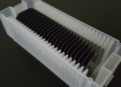
Silicon Wafer Si Wafer 8inch N Type P Type<111><100><110> SSP DSP Prime Grade Dummy Grade
Price: Negotiable
MOQ: Negotiable
Delivery Time: Negotiable
Brand: ZMSH
View More
Silicon wafer Si wafer 8inch N type P type SSP DSP Prime grade Dummy grade Product Overview: 8-Inch Prime Grade Silicon Wafer Silicon wafers are the backbone of the semiconductor industry, serving as the fundamental substrate for integrated circuits, microchips, and various electronic components. Th... View More
{"cid":"40149","pid":"50598668","pimg_url":"\/\/img1.ecerimg.com\/c9\/fb\/2e8a38b9eeeb\/product\/197016880_s-w400xh400.jpg","name":"Silicon Wafer Si Wafer 8inch N Type P Type<111><100><110> SSP DSP Prime Grade Dummy Grade","inquiry_url":"\/corp\/inquiry-new\/uu4zrn-1gbxac.html","attrs":{"Price":"Negotiable","MOQ":"Negotiable","Delivery Time":"Negotiable","Brand":"ZMSH"}}
Thermal Oxide Layer SiO2 Wafer Thickness 20um MEMS Optical Communication System
Price: Negotiable
MOQ: 5
Delivery Time: 2-4 weeks
Brand: ZMSH
View More
SiO2 wafer Thermal Oxide Laver Thickness 20um+5% MEMS Optical Communication System Product Description: The SIO2 silicon dioxide wafer serves as a foundational element in semiconductor manufacturing. Featuring a thickness ranging from 10μm to 25μm, this crucial substrate is available in 6-inch and 8... View More
{"cid":"40149","pid":"41385687","pimg_url":"\/\/img1.ecerimg.com\/c9\/fb\/2e8a38b9eeeb\/product\/161213127_s-w400xh400.jpg","name":"Thermal Oxide Layer SiO2 Wafer Thickness 20um MEMS Optical Communication System","inquiry_url":"\/corp\/inquiry-new\/uu4zrn-17jr8q.html","attrs":{"Price":"Negotiable","MOQ":"5","Delivery Time":"2-4 weeks","Brand":"ZMSH"}}
Large Thickness SiO2 Thermal Oxide On Silicon Wafers For Optical Communication System
Price: by quantites
MOQ: 10pcs
Delivery Time: 2-4weeks
Brand: ZMSH
View More
SapphiLarge Thickness Thermal Oxide (SiO2) On Silicon Wafers For Optical Communication System Generally, the oxide layer thickness of silicon wafers is mainly concentrated below 3um, and the countries and regions that can stably produce high-quality thick oxide layer (above 3um) silicon wafers are s... View More
{"cid":"40149","pid":"40330105","pimg_url":"\/\/img1.ecerimg.com\/c9\/fb\/2e8a38b9eeeb\/product\/157012916_s-w400xh400.jpg","name":"Large Thickness SiO2 Thermal Oxide On Silicon Wafers For Optical Communication System","inquiry_url":"\/corp\/inquiry-new\/uu4zrn-16jhds.html","attrs":{"Price":"by quantites","MOQ":"10pcs","Delivery Time":"2-4weeks","Brand":"ZMSH"}}
Beta Coefficient-Ga2O3 Gallium Oxide Wafer Doped Mg Fe3+ Square Substrate Dsp Ssp
Price: by case
MOQ: 5pcs
Delivery Time: in 30days
Brand: ZMKJ
View More
Gallium Oxide Epiwafers Beta Coefficient-Ga2O3 Gallium Oxide Wafer Doped Mg Fe3+ Square Substrate Dsp Ssp Properties of Ga2O3 β-Ga2O3 is a gallium oxide compound, which is a wide band gap semiconductor material. Its crystal structure belongs to the hexagonal crystal system, with high electron mobili... View More
{"cid":"40149","pid":"39167736","pimg_url":"\/\/img1.ecerimg.com\/c9\/fb\/2e8a38b9eeeb\/product\/154129333_s-w400xh400.jpg","name":"Beta Coefficient-Ga2O3 Gallium Oxide Wafer Doped Mg Fe3+ Square Substrate Dsp Ssp","inquiry_url":"\/corp\/inquiry-new\/uu4zrn-15f29r.html","attrs":{"Price":"by case","MOQ":"5pcs","Delivery Time":"in 30days","Brand":"ZMKJ"}}
300 - 900nm LN-On-Silicon LiNbO3 Lithium Niobate Wafer Thin Films Layer On Silicon Substrate
Price: by case
MOQ: 2pcs
Delivery Time: 4 weeks
Brand: ZMKJ
View More
300-900nm LN-On-Silicon LiNbO3 Lithium Niobate Wafer Thin Films Layer On Silicon Substrate Lithium niobate (LiNbO3) crystal is an important photoelectric material, and is widely used in integrated optics, nonlinear optics, optoelectronic components, and other fields, one of the most important substr... View More
{"cid":"40149","pid":"37906633","pimg_url":"\/\/img1.ecerimg.com\/c9\/fb\/2e8a38b9eeeb\/product\/150954699_s-w400xh400.jpg","name":"300 - 900nm LN-On-Silicon LiNbO3 Lithium Niobate Wafer Thin Films Layer On Silicon Substrate","inquiry_url":"\/corp\/inquiry-new\/uu4zrn-148jr9.html","attrs":{"Price":"by case","MOQ":"2pcs","Delivery Time":"4 weeks","Brand":"ZMKJ"}}
Large Size Optical Glass Sheet Windows Wafers D263 JGS2 JGS1 BF33 Material
Price: by case
MOQ: 3pcs
Delivery Time: 3-4weeks
Brand: zmkj
View More
custom 0.2mm~2mm bf33 glass sheet/borofloat 33 glass sheet High Temperature Resistance BF33/Fused Silica/Sapphire UV/IR Wavelength Optical Glass Sheet,Windows High Temperature Resistance BF33/Fused Silica/Sapphire UV/IR Wavelength Optical Glass Sheet,Windows fanshaped sapphire optical glass window,... View More
{"cid":"40149","pid":"36220289","pimg_url":"\/\/img1.ecerimg.com\/c9\/fb\/2e8a38b9eeeb\/product\/142802920_s-w400xh400.jpg","name":"Large Size Optical Glass Sheet Windows Wafers D263 JGS2 JGS1 BF33 Material","inquiry_url":"\/corp\/inquiry-new\/uu4zrn-12n3y1.html","attrs":{"Price":"by case","MOQ":"3pcs","Delivery Time":"3-4weeks","Brand":"zmkj"}}
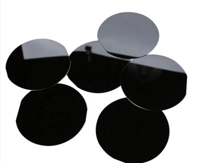
Quartz Wafer Quartz Wafers 2" 3" 4" 6" 8" 12" SiO₂ Semiconductor Optical
Price: 20USD
MOQ: 25
Delivery Time: 2-4 weeks
Brand: ZMSH
View More
Quartz Wafer Quartz Wafers 2", 3", 4", 6", 8", 12" SiO₂ Semiconductor Optical Introduction of Quartz Wafer Quartz wafers are made from crystalline silicon dioxide (SiO₂). The unique properties of quartz make it an essential material in various high-tech industries. Quar... View More
{"cid":"40149","pid":"53446428","pimg_url":"\/\/img1.ecerimg.com\/c9\/fb\/2e8a38b9eeeb\/product\/206404430_s-w400xh400.jpg","name":"Quartz Wafer Quartz Wafers 2\" 3\" 4\" 6\" 8\" 12\" SiO\u2082 Semiconductor Optical","inquiry_url":"\/corp\/inquiry-new\/uu4zrn-1k2taw.html","attrs":{"Price":"20USD","MOQ":"25","Delivery Time":"2-4 weeks","Brand":"ZMSH"}}
2" 3" 4" 6" 8" 12" SiO₂ Quartz Wafer Quartz Wafers SiO₂ MEMS Temperature
Price: 20USD
MOQ: 25
Delivery Time: 2-4 weeks
Brand: ZMSH
View More
Introduction Quartz wafers play an indispensable role in advancing the electronics, semiconductor, and optics industries. Found in smartphones guiding your GPS, embedded in high-frequency base stations powering 5G networks, and integrated into tools manufacturing next-gen microchips, quartz wafers a... View More
{"cid":"40149","pid":"53447603","pimg_url":"\/\/img1.ecerimg.com\/c9\/fb\/2e8a38b9eeeb\/product\/206407885_s-w400xh400.jpg","name":"2\" 3\" 4\" 6\" 8\" 12\" SiO\u2082 Quartz Wafer Quartz Wafers SiO\u2082 MEMS Temperature","inquiry_url":"\/corp\/inquiry-new\/uu4zrn-1k2vfk.html","attrs":{"Price":"20USD","MOQ":"25","Delivery Time":"2-4 weeks","Brand":"ZMSH"}}
LNOI Wafer 2/3/4/6/8 Inch LiNbO₃, Customizable Photonic Devices
Price: 1000USD
MOQ: 2
Delivery Time: 2-3 weeks
Brand: ZMSH
View More
LNOI Wafer 2/3/4/6/8 Inch (Si/LiNbO₃, Customizable) photonic devices Introduce of LNOI Wafer LiNbO3 Crystals is widely used as frequency doublers for wavelength > 1um and optical parametric oscillators (OPOs) pumped at 1064 nm as well as quasi-phase-matched (QPM) devices. Due to its large Elector... View More
{"cid":"40149","pid":"53384509","pimg_url":"\/\/img1.ecerimg.com\/c9\/fb\/2e8a38b9eeeb\/product\/206150082_s-w400xh400.jpg","name":"LNOI Wafer 2\/3\/4\/6\/8 Inch LiNbO\u2083, Customizable Photonic Devices","inquiry_url":"\/corp\/inquiry-new\/uu4zrn-1k0xvx.html","attrs":{"Price":"1000USD","MOQ":"2","Delivery Time":"2-3 weeks","Brand":"ZMSH"}}
LiTaO3 Wafer Lithium Tantalate Electro-Optic Nonlinear Optical Piezoelectric Customization
Price: Negotiable
MOQ: 2
Delivery Time: 2-4 weeks
Brand: ZMSH
View More
LiTaO3 Wafer Lithium Tantalate Electro-Optic Nonlinear Optical Piezoelectric Customization Introduce of LiTaO3 Wafer Lithium tantalate is an excellent multifunctional crystalline material characterized by its ilmenite-type structure, exhibiting a colorless or pale yellow appearance. Renowned for its... View More
{"cid":"40149","pid":"53261043","pimg_url":"\/\/img1.ecerimg.com\/c9\/fb\/2e8a38b9eeeb\/product\/205731391_s-w400xh400.jpg","name":"LiTaO3 Wafer Lithium Tantalate Electro-Optic Nonlinear Optical Piezoelectric Customization","inquiry_url":"\/corp\/inquiry-new\/uu4zrn-1jx59k.html","attrs":{"Price":"Negotiable","MOQ":"2","Delivery Time":"2-4 weeks","Brand":"ZMSH"}}