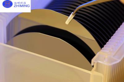
N-type SiC On Si Compound Wafer 6inch 150mm SiC Type 4H-N Si Type N Or P
Price: Negotiable
MOQ: 1
Delivery Time: 4-6 weeks
Brand: ZMSH
View More
N-type SiC on Si Compound Wafer 6inch 150mm SiC type 4H-N Si type N or P N-type SiC on Si Compound Wafer abstract N-type silicon carbide (SiC) on silicon (Si) compound wafers have garnered significant attention due to their promising applications in high-power and high-frequency electronic devices. ... View More
{"cid":"40149","pid":"47847786","pimg_url":"\/\/img1.ecerimg.com\/c9\/fb\/2e8a38b9eeeb\/product\/183544903_s-w400xh400.jpg","name":"N-type SiC On Si Compound Wafer 6inch 150mm SiC Type 4H-N Si Type N Or P","inquiry_url":"\/corp\/inquiry-new\/uu4zrn-1dqyxa.html","attrs":{"Price":"Negotiable","MOQ":"1","Delivery Time":"4-6 weeks","Brand":"ZMSH"}}
Silicon on Insulator SOI Wafer 6", 2.5 "m (P-doped ) + 1.0 SiO2 + 625um Si (P-type /Boron Doped )
Price: Negotiable
MOQ: 1
Delivery Time: 2-4 weeks
Brand: ZMSH
View More
Silicon-on-Insulator SOI wafer 6", 2.5 "m (P-doped ) + 1.0 SiO2 + 625um Si (P-type /Boron doped ) Silicon-on-Insulator (SOI) Wafer Abstract This Silicon-on-Insulator (SOI) wafer is a specialized semiconductor substrate designed for advanced electronic and microelectromechanical systems (ME... View More
{"cid":"40149","pid":"44939284","pimg_url":"\/\/img1.ecerimg.com\/c9\/fb\/2e8a38b9eeeb\/product\/171967072_s-w400xh400.jpg","name":"Silicon on Insulator SOI Wafer 6\", 2.5 \"m (P-doped ) + 1.0 SiO2 + 625um Si (P-type \/Boron Doped )","inquiry_url":"\/corp\/inquiry-new\/uu4zrn-1az6jm.html","attrs":{"Price":"Negotiable","MOQ":"1","Delivery Time":"2-4 weeks","Brand":"ZMSH"}}
SOI Wafer Silicon On Insulator 100mm 150mm P type Dopant B Device 220 Resistivity: 8.5-11.5 ohm-cm
Price: Negotiable
MOQ: 5
Delivery Time: 2-4 weeks
Brand: ZMSH
View More
SOI Wafer Silicon On Insulator 100mm 150mm P type Dopant B Device: 220 Resistivity: 8.5-11.5 ohm-cm Product Detail Page for SOI Wafer (Silicon-On-Insulator) Product Overview Introducing our high-performance Silicon-On-Insulator (SOI) wafers, available in 100mm and 150mm diameters. These wafers are e... View More
{"cid":"40149","pid":"44939944","pimg_url":"\/\/img1.ecerimg.com\/c9\/fb\/2e8a38b9eeeb\/product\/171967271_s-w400xh400.jpg","name":"SOI Wafer Silicon On Insulator 100mm 150mm P type Dopant B Device 220 Resistivity: 8.5-11.5 ohm-cm","inquiry_url":"\/corp\/inquiry-new\/uu4zrn-1az778.html","attrs":{"Price":"Negotiable","MOQ":"5","Delivery Time":"2-4 weeks","Brand":"ZMSH"}}
SOI Wafer Silicon On Insulator Wafer Dopant P BOX Layer 0.4-3 Substrate Orientation 100 111
Price: Negotiable
MOQ: 1
Delivery Time: 2-4 weeks
Brand: ZMSH
View More
SOI Wafer Silicon On Insulator wafer Dopant P BOX Layer 0.4-3 Substrate Orientation 100 111 SOI wafer‘s abstract SOI (Silicon-On-Insulator) wafers are a type of semiconductor material technology used primarily in the microelectronics industry. These wafers are constructed by inserting a thin layer o... View More
{"cid":"40149","pid":"44940005","pimg_url":"\/\/img1.ecerimg.com\/c9\/fb\/2e8a38b9eeeb\/product\/171967403_s-w400xh400.jpg","name":"SOI Wafer Silicon On Insulator Wafer Dopant P BOX Layer 0.4-3 Substrate Orientation 100 111","inquiry_url":"\/corp\/inquiry-new\/uu4zrn-1az795.html","attrs":{"Price":"Negotiable","MOQ":"1","Delivery Time":"2-4 weeks","Brand":"ZMSH"}}
2inch Silicon Wafers P-type N-type CZ Growth Method BOW ≤30 For LED Lighting
Price: Negotiable
MOQ: 1
Delivery Time: 2-4 weeks
Brand: ZMSH
View More
2inch silicon wafers p-type n-type CZ growth method BOW ≤30 for LED lighting Silicon wafers' abstract Silicon wafers are the foundational material used in the semiconductor industry for the fabrication of integrated circuits and various microdevices. Made from highly purified silicon, these wafers s... View More
{"cid":"40149","pid":"44940037","pimg_url":"\/\/img1.ecerimg.com\/c9\/fb\/2e8a38b9eeeb\/product\/171967478_s-w400xh400.jpg","name":"2inch Silicon Wafers P-type N-type CZ Growth Method BOW \u226430 For LED Lighting","inquiry_url":"\/corp\/inquiry-new\/uu4zrn-1az7a5.html","attrs":{"Price":"Negotiable","MOQ":"1","Delivery Time":"2-4 weeks","Brand":"ZMSH"}}
Silicon Wafer N Type P Dopant 2inch 4inch 6inch 8inch Resistivity 0-100 Ohm-cm Single Side Polished
Price: Negotiable
MOQ: Negotiable
Delivery Time: Negotiable
Brand: ZMSH
View More
Silicon wafer N type P Dopant 2inch 4inch 6inch 8inch Resistivity: 0-100 ohm-cm Single side polished Product abstract Silicon wafers are thin slices of semiconductor material, predominantly silicon, used as the substrate in the manufacture of integrated circuits (ICs) and other microelectronic devic... View More
{"cid":"40149","pid":"44940047","pimg_url":"\/\/img1.ecerimg.com\/c9\/fb\/2e8a38b9eeeb\/product\/171967550_s-w400xh400.jpg","name":"Silicon Wafer N Type P Dopant 2inch 4inch 6inch 8inch Resistivity 0-100 Ohm-cm Single Side Polished","inquiry_url":"\/corp\/inquiry-new\/uu4zrn-1az7af.html","attrs":{"Price":"Negotiable","MOQ":"Negotiable","Delivery Time":"Negotiable","Brand":"ZMSH"}}
3inch InP Indium Phosphide Substrate N-Type Semiconductor VGF Growth Method 111 100 Orientation
Price: Negotiable
MOQ: Negotiable
Delivery Time: 2-4 weeks
Brand: ZMSH
View More
3inch InP Indium Phosphide Substrate N-Type Semiconductor VGF growth method 000 001 orientation Product abstract Our InP (Indium Phosphide) products offer high-performance solutions for a variety of applications in the telecommunications, optoelectronics, and semiconductor industries. With superior ... View More
{"cid":"40149","pid":"43888357","pimg_url":"\/\/img1.ecerimg.com\/c9\/fb\/2e8a38b9eeeb\/product\/169777171_s-w400xh400.jpg","name":"3inch InP Indium Phosphide Substrate N-Type Semiconductor VGF Growth Method 111 100 Orientation","inquiry_url":"\/corp\/inquiry-new\/uu4zrn-19z495.html","attrs":{"Price":"Negotiable","MOQ":"Negotiable","Delivery Time":"2-4 weeks","Brand":"ZMSH"}}
Silicon Wafer 4 Inch Thickness 500+/-20 Resistivity 1-10 Ohm·cm Orientation100 Double Side Polish
Price: Negotiable
MOQ: Negotiable
Delivery Time: Negotiable
Brand: ZMSH
View More
Silicon wafer 4 inch thickness 500+/-20 Resistivity 1-10 ohm·cm Orientation100 double side polish Product abstract Our Precision Ultra-Pure Silicon Substrate is meticulously engineered to serve as the foundation for high-performance semiconductor devices. Crafted with advanced float-zone mono-crysta... View More
{"cid":"40149","pid":"43888652","pimg_url":"\/\/img1.ecerimg.com\/c9\/fb\/2e8a38b9eeeb\/product\/169784219_s-w400xh400.jpg","name":"Silicon Wafer 4 Inch Thickness 500+\/-20 Resistivity 1-10 Ohm\u00b7cm Orientation100 Double Side Polish","inquiry_url":"\/corp\/inquiry-new\/uu4zrn-19z4jc.html","attrs":{"Price":"Negotiable","MOQ":"Negotiable","Delivery Time":"Negotiable","Brand":"ZMSH"}}
Silicon Wafer CZ orientation111 Resistivity: 1-10 (ohm.cm) single side or double side polish
Price: Negotiable
MOQ: Negotiable
Delivery Time: Negotiable
Brand: ZMSH
View More
Silicon Wafer CZ orientation111 Resistivity: 1-10 (ohm.cm) single side or double side polish Product abstract Our Si wafer offers high purity and exceptional uniformity, ideal for a wide range of semiconductor and photovoltaic applications. With precise control over crystal structure and surface qua... View More
{"cid":"40149","pid":"43888719","pimg_url":"\/\/img1.ecerimg.com\/c9\/fb\/2e8a38b9eeeb\/product\/169784863_s-w400xh400.jpg","name":"Silicon Wafer CZ orientation111 Resistivity: 1-10 (ohm.cm) single side or double side polish","inquiry_url":"\/corp\/inquiry-new\/uu4zrn-19z4mf.html","attrs":{"Price":"Negotiable","MOQ":"Negotiable","Delivery Time":"Negotiable","Brand":"ZMSH"}}
Epi Ready 4inch InP Wafers N Type P Type EPF<1000cm^2 With The Thickness Of 325um±50um
Price: Negotiable
MOQ: Negotiable
Delivery Time: Negotiable
Brand: ZMSH
View More
Epi ready 4inch InP wafers N-type p-type EPF<1000cm^2 with the thickness of 325um±50um Product abstract Our product, the "High-Purity Indium Phosphide (InP) Wafer," stands at the forefront of semiconductor innovation. Crafted from pristine indium phosphide, a binary semiconductor renowned ... View More
{"cid":"40149","pid":"43887011","pimg_url":"\/\/img1.ecerimg.com\/c9\/fb\/2e8a38b9eeeb\/product\/169775539_s-w400xh400.jpg","name":"Epi Ready 4inch InP Wafers N Type P Type EPF\uff1c1000cm^2 With The Thickness Of 325um\u00b150um","inquiry_url":"\/corp\/inquiry-new\/uu4zrn-19z2z3.html","attrs":{"Price":"Negotiable","MOQ":"Negotiable","Delivery Time":"Negotiable","Brand":"ZMSH"}}
Single Crystal Si Wafer Electronic Device Substrate Photolithography Layer 2"3"4"6"8"
Price: Negotiable
MOQ: 10
Delivery Time: 2-4 weeks
Brand: ZMSH
View More
Product Description: A silicon wafer, often referred to as a Si wafer, is a fundamental component in the semiconductor industry, playing a crucial role in the fabrication of electronic devices. Silicon, a semiconductor material, is used to manufacture these wafers due to its excellent electrical pro... View More
{"cid":"40149","pid":"42235717","pimg_url":"\/\/img1.ecerimg.com\/c9\/fb\/2e8a38b9eeeb\/product\/165087315_s-w400xh400.jpg","name":"Single Crystal Si Wafer Electronic Device Substrate Photolithography Layer 2\"3\"4\"6\"8\"","inquiry_url":"\/corp\/inquiry-new\/uu4zrn-18cpc5.html","attrs":{"Price":"Negotiable","MOQ":"10","Delivery Time":"2-4 weeks","Brand":"ZMSH"}}
High Purity Silicon Wafer Conductivity Solar Cells Power Semiconductor Devices
Price: Negotiable
MOQ: 5
Delivery Time: 2-4 weeks
Brand: ZMSH
View More
Silicon wafer Conductivity Solar Cells Solar Cells Power Semiconductor Devices High Purity Product Description: Attributes Details Substrate Material Single Crystal Silicon Wafer Primary Flat Orientation +/-1 Deg Secondary Flat Orientation 90 Deg From Primary Flat Diameter 100 Mm +/- 0.5 Mm Oxygen C... View More
{"cid":"40149","pid":"42235808","pimg_url":"\/\/img1.ecerimg.com\/c9\/fb\/2e8a38b9eeeb\/product\/165096967_s-w400xh400.jpg","name":"High Purity Silicon Wafer Conductivity Solar Cells Power Semiconductor Devices","inquiry_url":"\/corp\/inquiry-new\/uu4zrn-18cpf0.html","attrs":{"Price":"Negotiable","MOQ":"5","Delivery Time":"2-4 weeks","Brand":"ZMSH"}}
4 Inches 6 Inches 8 Inches SOI Wafers Compatible With CMOS Three Layer Structure
Price: Negotiable
MOQ: 5
Delivery Time: 2-4 weeks
Brand: ZMSH
View More
SOI wafers 4 Inches, 6 Inches, 8 Inches, Compatible with CMOS three-layer structure Product Description: The SOI (Silicon on Insulator) wafer stands as a pioneering marvel in the realm of semiconductor technology, revolutionizing the landscape of advanced electronics. Comprising three distinct layer... View More
{"cid":"40149","pid":"41458150","pimg_url":"\/\/img1.ecerimg.com\/c9\/fb\/2e8a38b9eeeb\/product\/161401513_s-w400xh400.jpg","name":"4 Inches 6 Inches 8 Inches SOI Wafers Compatible With CMOS Three Layer Structure","inquiry_url":"\/corp\/inquiry-new\/uu4zrn-17mz16.html","attrs":{"Price":"Negotiable","MOQ":"5","Delivery Time":"2-4 weeks","Brand":"ZMSH"}}
6 Inch 8 Inch SIO2 Silicon Dioxide Wafer Thickness 10um-25um Surface Micromachining
Price: Negotiable
MOQ: 5
Delivery Time: Negotiable
Brand: ZMSH
View More
6 inch 8 inch SIO2 silicon dioxide wafer thickness 20um 10um-25um Crystal Substrate Product Description: The SIO2 silicon dioxide wafer, vital in semiconductor production, features a thickness ranging from 10μm to 25μm and is available in 6-inch and 8-inch diameters. Primarily serving as an essentia... View More
{"cid":"40149","pid":"41385673","pimg_url":"\/\/img1.ecerimg.com\/c9\/fb\/2e8a38b9eeeb\/product\/161212515_s-w400xh400.jpg","name":"6 Inch 8 Inch SIO2 Silicon Dioxide Wafer Thickness 10um-25um Surface Micromachining","inquiry_url":"\/corp\/inquiry-new\/uu4zrn-17jr89.html","attrs":{"Price":"Negotiable","MOQ":"5","Delivery Time":"Negotiable","Brand":"ZMSH"}}
High Purity Silicon Wafers High Thermal Conductivity 3 Inch 4 Inch 6 Inch 8 Inch
Price: Negotiable
MOQ: 10
Delivery Time: 2-4 weeks
Brand: ZMSH
View More
Electronic-Grade Silicon Wafers Ultra-High Purity Optoelectronic-Grade Abstract The high-purity silicon wafer we offer undergoes precision machining and strict quality control, meeting the semiconductor industry's high demands for purity and performance. These wafers are made from pure raw materials... View More
{"cid":"40149","pid":"41233979","pimg_url":"\/\/img1.ecerimg.com\/c9\/fb\/2e8a38b9eeeb\/product\/160855558_s-w400xh400.jpg","name":"High Purity Silicon Wafers High Thermal Conductivity 3 Inch 4 Inch 6 Inch 8 Inch","inquiry_url":"\/corp\/inquiry-new\/uu4zrn-17e43v.html","attrs":{"Price":"Negotiable","MOQ":"10","Delivery Time":"2-4 weeks","Brand":"ZMSH"}}
GaP Wafer Gallium Phosphide Single Crystal Orientation (111)A 0°±0.2 Solar Cells
Price: Negotiable
MOQ: Negotiable
Delivery Time: Negotiable
Brand: ZMSH
View More
GaP Wafer, Gallium Phosphide single crystal Orientation (111)A 0°±0.2 Solar Cells Product Description: Gallium Phosphide GaP, an important semiconductor of unique electrical properties as other III-V compound materials, crystallizes in the thermodynamically stable cubic ZB structure, is an orange-ye... View More
{"cid":"40149","pid":"41397887","pimg_url":"\/\/img1.ecerimg.com\/c9\/fb\/2e8a38b9eeeb\/product\/161249855_s-w400xh400.jpg","name":"GaP Wafer Gallium Phosphide Single Crystal Orientation (111)A 0\u00b0\u00b10.2 Solar Cells","inquiry_url":"\/corp\/inquiry-new\/uu4zrn-17k45z.html","attrs":{"Price":"Negotiable","MOQ":"Negotiable","Delivery Time":"Negotiable","Brand":"ZMSH"}}
2inch GaP Wafer With OF Location/Length EJ 0-1-1 / 16±1mm LED LD Mobility Min 100
Price: Negotiable
MOQ: 5
Delivery Time: 2-4 weeks
Brand: ZMSH
View More
GaP wafer 2inch with OF Location/Length EJ 0-1-1 / 16±1mm LED LD Mobility Min 100 Product Description: A GaP wafer is a semiconductor substrate primarily used in the fabrication of various electronic and optoelectronic devices. Gallium Phosphide (GaP) wafers exhibit exceptional optical and electroni... View More
{"cid":"40149","pid":"41397886","pimg_url":"\/\/img1.ecerimg.com\/c9\/fb\/2e8a38b9eeeb\/product\/161249682_s-w400xh400.jpg","name":"2inch GaP Wafer With OF Location\/Length EJ 0-1-1 \/ 16\u00b11mm LED LD Mobility Min 100","inquiry_url":"\/corp\/inquiry-new\/uu4zrn-17k45y.html","attrs":{"Price":"Negotiable","MOQ":"5","Delivery Time":"2-4 weeks","Brand":"ZMSH"}}
Semi Insulating GaN-On-Silicon Wafer Free Standing Gallium Nitride Substrates
Price: by case
MOQ: 3pcs
Delivery Time: 2-4weeks
Brand: zmkj
View More
Gallium Nitride Substrates GaN Wafers GaN-On-Silicon Free-Standing Substrate Semi-insulting We can offer 2 to 8-inch gallium nitride (GaN) single crystal substrate or epitaxial sheet, and sapphire/silicon-based 2 to 8-inch GaN epitaxial sheets are available. The rapid development of the first and se... View More
{"cid":"40149","pid":"40177566","pimg_url":"\/\/img1.ecerimg.com\/c9\/fb\/2e8a38b9eeeb\/product\/156401973_s-w400xh400.jpg","name":"Semi Insulating GaN-On-Silicon Wafer Free Standing Gallium Nitride Substrates","inquiry_url":"\/corp\/inquiry-new\/uu4zrn-16dwey.html","attrs":{"Price":"by case","MOQ":"3pcs","Delivery Time":"2-4weeks","Brand":"zmkj"}}
Y-42 Degree 4inch Lithium Tantalate LiTaO3 LiNbO3 Lithium Niobate Crystal Raw Unprocessed Ingots
Price: by case
MOQ: 1pcs
Delivery Time: 3-10days
Brand: ZMSH
View More
Y-42° LT 4inch Lithium Tantalate LiTaO3 LiNbO3 Lithium Niobate Crystal Raw Unprocessed Ingots Product Description: 1, lithium tantalate is a chemical substance, chemical formula LiTaO3. Colorless or yellowish crystal. Tripartite system, distorted perovskite type structure, point group C63vR3C. Densi... View More
{"cid":"40149","pid":"37794943","pimg_url":"\/\/img1.ecerimg.com\/c9\/fb\/2e8a38b9eeeb\/product\/150414072_s-w400xh400.jpg","name":"Y-42 Degree 4inch Lithium Tantalate LiTaO3 LiNbO3 Lithium Niobate Crystal Raw Unprocessed Ingots","inquiry_url":"\/corp\/inquiry-new\/uu4zrn-1455nz.html","attrs":{"Price":"by case","MOQ":"1pcs","Delivery Time":"3-10days","Brand":"ZMSH"}}
InAs Wafer Crystal Substrates N Type For MBE 99.9999% Monocrystalline
Price: by case
MOQ: 3pcs
Delivery Time: 2-4weeks
Brand: zmkj
View More
2inch 3inch 4inch InAs Wafer Crystal Substrates N-Type For MBE 99.9999% Monocrystalline Introduce of InAs substrateIndium InAs or indium mono-arsenide is a semiconductor composed of indium and arsenic. It has the appearance of a gray cubic crystal with a melting point of 942°C. Indium arsenide is us... View More
{"cid":"40149","pid":"37935129","pimg_url":"\/\/img1.ecerimg.com\/c9\/fb\/2e8a38b9eeeb\/product\/151085070_s-w400xh400.jpg","name":"InAs Wafer Crystal Substrates N Type For MBE 99.9999% Monocrystalline","inquiry_url":"\/corp\/inquiry-new\/uu4zrn-149ejs.html","attrs":{"Price":"by case","MOQ":"3pcs","Delivery Time":"2-4weeks","Brand":"zmkj"}}